Quantcast
Channel: BALD Engineering - Born in Finland, Born to ALD
Viewing all 1586 articles
Browse latest View live

Picosun to deliver the first ALD tools to Africa at University of Johannesburg

$
0
0
[IT-Online LINK] For the first time ever, a pathway for ALD-enhanced materials to be rapidly developed and transitioned in a University of Johannesburg laboratory will be available for nearly any application. The laboratory construction is a natural next step in implementing the strategy to establish national nanotechnology in South Africa.

UJ aims to lead the world’s research and development on cutting edge nanomaterial fabrication technology. A major nanofabrication facility housing world class ALD reactors at the School of Mechanical & Industrial Engineering last week broke ground for construction within the Department of Mechanical Engineering Science at the Auckland Park Kingsway Campus (APK).

The University of Johannesburg’s Faculty of Engineering and the Built Environment (FEBE) is looking forward to the new Atomic Layer Deposition (ALD) cleanroom facility that will transform the South African economy while also ensuring that cutting-edge and high quality learning opportunities are on offer.

The establishment of the Atomic Layer Deposition (ALD) cleanroom facility will assist in providing academics with the ability to manage material properties at an atomic level. The desired materials with preferred nano-structure can be assembled by applying layers of atoms/molecules on the substrate to simultaneously achieve the required level of performance and precise parameter control. Practical applications of nanotechnology include the use of ALD ultrathin films in, for example, photovoltaics, optical coatings, barrier coatings to protect against tarnish and corrosion, and in a variety of semiconductors, superconductors, and flexible electronics.

The project, scheduled to finish in four months, is one of the country’s major mega engineering facilities in Africa.

“This is an incredibly exciting time for the Faculty of Engineering,” says Professor Daniel Mashao, Executive Dean: Faculty of Engineering and the Built Environment (FEBE). “The building will be spectacular and we’ll be doing great science here very soon as we have the space and infrastructure to grow and do research in a way we simply couldn’t do before.”

“This additional laboratory space, designed specifically to encourage the kind of interdisciplinary research UJ is known for, will be critical to growing the school’s research enterprise,” says Dr Daniel Madyira, Acting Head of Department (HOD): Mechanical Engineering Science, at the groundbreaking ceremony.

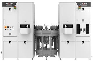
Professor Tien-Chien Jen, the substantive Head of the Department of Mechanical Engineering who is currently on an international expedition in the USA, spearheads the project. This ALD cleanroom facility with the two state-of-the-art reactors (R-200 and R-200 advance supplied by Picosun, Oy) were funded by NRF NEP (National Equipment Program) and IBP (Infrastructure Bridge Program) with a total funding around R18 million.

“This project is a critical step in the Institution’s vision of the 4.0 future, providing the technological basis for the construction of a cleanroom laboratory, which will assist our engineers when they use special ‘sub-nano-scopic’ techniques that allow the manufacturing of individual ultra-thin films on the surface with atomic scale deposition precision and nearly prefectcomformality. This facility will illustrate a better understanding of the way that atoms/molecules move together to synthesise the new and functionalised materials, that may have major impacts on our ability to design and use these new nanostructure materials for vast applications in the fields of energy, materials, medical devices semi-conductors etc,” explains Dr Mashao.

This ALD cleanroom facility will provide an ultra-low number of particle (ISO-7) and nearly vibration- free environment for the two state-of-the-art ALD reactors (Picosun R-200 and R-200 advance), which allow the engineering squad to study numerous states and properties of various unique new nanomaterials at the atomic scale. It will be a unique building in Africa and seeks to lead the world in state-of-the-art research on nanotechnology.

Construction is expected to be finished by September 2019 and reactors installation and advance training will be provided by Picosun and is expected to be completed by the end of October. The ALD cleanroom facility will be fully functional in November 2019.

Laboratory activities will be aimed at offering a wide range of services: ALD applied research studies, demonstrating ALD opportunities, integrating ALD into various industries, implementing international ALD experience, manufacturing and analysing samples, coating services and pilot manufacturing, as well as technology training and applying ALD equipment.

Picosun launches a new ALD product platform for up to 200 mm wafer markets

$
0
0
SEMICON West, SAN FRANCISCO, CA, USA, 9th July 2019– Picosun Group, the leading provider of AGILE ALD™ (Atomic Layer Deposition) thin film coating solutions, has launched PICOSUN™ Morpher, a new ALD product platform designed to disrupt the up to 200 mm wafer markets in Beyond and More than Moore domains.

The PICOSUN™ Morpher ALD platform enables fast, cost-efficient, high volume production of e.g. MEMS, sensors, LEDs, lasers, power electronics, optics, and 5G components with the leading process quality, reliability, and operational agility.


“Morpher starts a completely new era in PICOSUN™ products, enabling the most advanced devices and components for IoT, 5G communications, autonomous transportation, AR and VR, to name just a few end applications,” states Dr. Jani Kivioja, CTO of Picosun Group.


Morpher adapts to the changing needs of different business verticals, from corporate R&D to production and foundry manufacturing. Unmatched versatility in substrate materials, substrate and batch size, and the comprehensive process range make Morpher truly a transformable, all-inclusive manufacturing facility for a wide range of semiconductor industries. The SEMI certified PICOSUN™ Morpher comes with completely new software where intuitive and user-friendly HMI allows unified control of the whole cluster.

“Morpher’s flexibility and adaptability, combined with the latest design attributes and the state-of-the-art software truly manifest our slogan ‘Agile ALD’. Together with our comprehensive consultancy, knowledge transfer and lifecycle management services we provide our customers a genuinely strategic partnership to keep them at the cutting edge of their industries,” continues Dr. Kivioja.


RASIRC Utilizes Novel Safe Hydrazine Delivery System to Enable Low Temperature Group III Metal-Nitride Deposition

$
0
0
Company presents AlN deposition results at International Conference on Nitride Semiconductors

San Diego, Calif – July 8, 2019 – RASIRC will discuss the benefits of anhydrous hydrazine as a nitrogen source at the 13th International Conference on Nitride Semiconductors (ICNS-13) in Bellevue, WA on July 7–12. RASIRC Chief Technology Officer Dr. Daniel Alvarez will present “Low Temperature Aluminum Nitride Deposition Enabled by Hydrazine” during the event’s poster session on Tuesday July 9. The poster will compare growth characteristics and film properties for TMA/Brute Hydrazine versus TMA/Ammonia. 
“To date, low temperature III-Nitride deposition has been plagued by low growth rates and unwanted residual carbon and hydrogen remaining from precursor materials. Utilization of hydrazine is thermodynamically more favorable due to the reactive nature of the N-N bond,” says Alvarez. “Hydrazine has been around for many years, but is only now ready for III-Nitride manufacturing thanks to safety and contamination issues addressed by RASIRC.”

RASIRC President and Founder Jeffrey Spiegelman adds, “The use of hydrazine will enable our customers to have larger process windows while reducing costly precursor consumption found with sources like Indium.”

ICNS-13 will present high-impact scientific and technological advances in materials and devices based on group-III nitride semiconductors, and will feature plenary sessions, parallel topical sessions, poster sessions and an industrial exhibition. The ICNS-13 Exhibit offers the most direct access to researchers from around the world who are seeking technical solutions to their challenges.

Dr. Alvarez will be available at ICNS-13 to discuss the RASIRC precursor chemistry product line-up, which includes hydrazine, hydrogen peroxide and more. Information about RASIRC products will also be available in the Matheson Gas exhibition booth.

About RASIRC Products

BRUTE® Hydrazine enables uniform nitride deposition for Silicon and Group III metals at low temperature. BRUTE Hydrazine may also be used as an atomic hydrogen source, where metals such as Ru, Cu, and Co may be cleaned and reduced. Hydrazine gas is generated in situ and is virtually water free. Brute Hydrazine has been formulated for a relatively high flash point for safer handling.

BRUTE Peroxide is a novel oxidant that improves nucleation density at film interfaces when compared to other oxidants. Surface functionalization is more dense and initiation is faster using anhydrous hydrogen peroxide gas compared with alternatives. This enables better selectivity and less damage to metal surfaces in ASD processes.

RASIRC Peroxidizer® provides high volumes of reactive H2O2/H2O mixtures for high throughput ALD. This reactive gas generator is ideal for roll-to-roll ALD coatings that require high speed deposition at reduced temperatures. Additional RASIRC products include the RainMaker® Humidification System (RHS) and the Hydrogen Peroxide Steamer (HPS). The RHS generates water vapor for oxidation applications and the HPS provides surface cleaning, preconditioning, wet thermal oxidation and residual carbon removal.

Endura Impulse - Applied Materials’ New Memory Machines

$
0
0

Tools designed to rapidly build embedded MRAM, RRAM, and phase change memories on logic chips expand foundry options

Applied Materials unveiled Endura Impulse System incorporating nine physical vapor deposition reactors to rapidly build STT-MRAM, RRAM or PCRAM, on 9 July at Semicon West, in San Francisco.
Chip equipment giant Applied Materials wants foundry companies to know that it feels their pain. Continuing down the traditional Moore's Law path of increasing the density of transistors on a chip is too expensive for all but the three richest players—Intel, Samsung, and TSMC. So to keep the customers coming, other foundries can instead add new features, such as the ability to embed new non-volatile memories—RRAM, phase change memory, and MRAM—right on the processor. 
The trouble is, those are really hard things to make at scale. So, Applied has invented a pair of machines that boost throughput by more than an order of magnitude.


Applied Materials' Endura Impulse uses nine physical vapor deposition systems to rapidly build RRAM or PCRAM. Photo: Applied Materials 
Source: Applied Materials LINK
----------
By Abhishekkumkar Thakur 

In Situ Cu Surface Cleaning with Anhydrous Hydrazine highlighted at AVS ALD 2019 by University of Texas at Dallas and RASIRC

$
0
0
Copper replaced Aluminum for interconnects in the semiconductor industry due to its low resistivity, high resistance to electromigration, low temperature coefficient of resistance, and good thermal stability [1].

Due to the lack of volatile copper compounds, copper could not be patterned by the techniques of photoresist masking and plasma etching that had been used for aluminum. The inability to plasma etch copper meant that the whole metal patterning process had to be redesigned and the result was a process referred to as an additive patterning, also known as a "Damascene" or "dual-Damascene" process by analogy to a traditional technique of metal inlaying. [2]

However, the exposed Cu interconnects during via-opening and post CMP process are vulnerable to oxidation with water rinse and exposure to air, resulting in reliability degradation [3]. Therefore, additional process for reduction of copper oxide should be required. The cleaning of copper can be achieved by either physical Ar sputtering or chemical reduction process [4]. Recent demonstration of chemical-based cleaning of Cu interconnects is expected to overcome disadvantages of physical Ar sputtering process, such as chamfering and re-deposition on vias and trenches. A number of studies on vapor-based reduction of copper oxide under ambient pressure conditions and at temperatures below 350 °C using hydrogen, ammonia, carbon monoxide, forming gas, acetic acid, formic acid, and ethanol as reducing agents have been reported [5,6]. On the other hand, Hydrazine (N2H4) can be used in the reduction of copper oxide due to its higher reduction capability [7].

Inspired by hydrazine’s unique characteristics, University of Texas at Dallas and RASIRC have explored the feasibility of vapor-phase reduction of copper oxide using anhydrous N2H4 to achieve an ideal metallic Cu film in an ALD environment.


Figure 1. Schematic of (a) RTALD system, (b) Process sequence, and (c) representative time sequence of stop valve process.

In summary, it could be shown that following an ozone treatment (Figure 1) a N2H4 treatment could effectively reduce the Cu2O to metallic Cu(0) from 150 – 200 oC. In addition, there was no detection of intermediate materials (e.g. Cu3N, Cu(OH)2, CuH, etc.). The following possible thermodynamic reaction is given CuO + Cu2O + N2H4 à 3Cu + 2H2O(g) + N2(g)

The details of the study will be presented at AVS ALD2019 and future work will be on potential application to Ru and Co cleaning/reduction, which have become important interconnect metals for 14/16 nm Logic and below, especially at the highly scaled lower metallization levels (M0 to M4).

References

1. R. P. Chaukulkar, N. F. W. Thissen, V. R. Rai, and S. Agarwal, J. Vac. Sci. Technol. A, 32, 01A108 (2014).
2. Copper interconnects, Wikipedia LINK: https://en.wikipedia.org/wiki/Copper_interconnects
3. Y.-L. Cheng, C.-Y. Lee, and Y.-L. Huang, in Noble and Precious Metals-Properties, Nanoscale Effects and Applications, M. Seehar and A. Bristow, Editors, p. 216–250, Intechopen (2018).
4. C. K. Hu et al., Microelectron. Eng., 70, 406–411 (2003).
5. L. F. Pena, J. F. Veyan, M. A. Todd, A. Derecskei-Kovacs, and Y. J. Chabal, ACS Appl. Mater. Interfaces, 10, 38610–38620 (2018).
6. Y. Chang, J. Leu, B.-H. Lin, Y.-L. Wang, and Y.-L. Cheng, Adv. Mater. Sci. Eng., 2013, 1–7 (2013).
7. D. M. Littrell, D. H. Bowers, and B. J. Tatarchuk, J. Chem. Soc. Faraday Trans. 1 Phys. Chem. Condens. Phases, 83, 3271–3282 (1987).


Beneq unveils R2, a compact modular platform for ALD research and application development

$
0
0

Modular Design and Attractive Price Point Make Advanced ALD Research More Accessible Than Ever


The new Beneq R2 is physically unveiled at the Beneq showroom (3rd floor) of the ALD 2019 conference in Bellevue WA, between July 22-24.


Bellevue, Washington, USA – Beneq today unveiled R2, a compact modular platform that makes it dramatically easier for universities, research institutes and enterprises to start advanced ALD research. Completely redesigned from the ground up with ergonomics in mind, the basic R2 model comes fully equipped for thermal ALD. With flexible add-on options customers can easily expand to other advanced processes such as plasma, batch processing, powder ALD, and reduced flow.


Hear the story behind the product, from the team who created the Beneq R2.

For researchers entering the rapidly growing domain of ALD research, the investment in equipment has always been subject to great uncertainty. Academic researchers find themselves having to choose between a beginner’s system with heavily limited capabilities or a full-fledged system at a prohibitive price – often diminishing available budgets.

The R2 system is designed to offer full features of thermal ALD, at a compact enclosure and an attractive price point. Built with all industry-standard equipment, the R2 delivers outstanding value whether you are experimenting in ALD research, process engineering or application development. It is designed by the same team of experts who created the TFS 200, the premium clusterable ALD research tool preferred by universities and researchers worldwide. “The Beneq R2 carries the same heritage and know-how that has made Beneq the leader in ALD for the last 25 years,” said Patrick Gonzalez, Beneq’s Technical Sales Manager. “The basic R2 system comes configured right out of the box, so you can experiment with encapsulation, high k-dielectrics, and everything in between.”


Ergonomic Design


To create a minimalist product that is easy to use, Beneq completely redesigned the physical look of the R2. To minimize the amount of piping required, the R2’s liquid sources are made extremely compact and placed close to the vacuum chamber. Unlike conventional designs heat source cabinets are repositioned right next to the vacuum chamber at a convenient height, making it easier than ever to replace containers and operate the tool. On the R2 Beneq has created a patent-pending air-cooling system over the vacuum chamber, minimizing the risk of overheating and avoiding unintended injuries.

Easy Upgrades


With a revolutionary modular design the Beneq R2 offers customers a suite of expansion options for the vacuum chamber, hot sources, or process types such as reduced flow for high-aspect ratio structures. Users can select their own configuration when placing a new order, or choose to upgrade the tool later. To learn more, visit www.beneq.com/r2.


About Beneq


Beneq is the home of ALD, offering a wide portfolio of equipment products and development services. Today Beneq leads the market with innovative solutions for advanced R&D (TFS 200, R2), flexible high-volume manufacturing (ALD 3, ALD 4), ultra-fast high precision spatial ALD coatings (C2R), roll-to-roll thin film coating of continuous webs (WCS 600), and specialized batch production for thicker film stacks (P400, P800). Headquartered in Espoo, Finland Beneq is dedicated to making ALD technology accessible for researchers and providing the invisible advantage in emerging semiconductor applications.


Press Contact

Lie Luo

Beneq

lie.luo@beneq.com


Strem offer hafnium metal alkylamide ALD precursors for emerging memory applications

$
0
0

Having been extensively studied over three decades for the replacement of silicon dioxide (SiO2) in conventional semiconductor fabrication, ALD Hafnium Oxide (HfO2) among other high-k dielectrics was finally adopted by Samsung in 2004 in high volume manufacturing at the 90 nm DRAM node as the high-k capacitor dielectric. The other DRAM companies followed, and later in 2007 Intel introduced ALD HfO2 at the 45 nm node as high-k gate dielectric. On account of its high dielectric constants (at least four times that of silicon dioxide) a thicker film of hafnium oxide can be used to achieve the same dielectric performance resulting from a thinner silicon dioxide layer without the associated high leakage current or even electron tunneling for ultra-thin dielectrics. High refractory oxides such as those of zirconium and hafnium also find uses in optical applications; as catalysts; and, because of their hardness and thermal stability, as protective coatings.


In recent years, hafnium oxide (as well as doped and oxygen-deficient hafnium oxide) has attracted additional interest as a possible candidate for resistive-switching memories (ReRAM) and CMOS-compatible ferroelectric field effect transistors and memory chips. A great example is Dresden based NaMLab and The Ferroelectric Memory Company (FMC) who are integrating HfO2 based ferroelectric transistor (FeFET) memory. The FeFET is a long-term contender for an ultra-fast, low-power, and non-volatile memory technology. In these devices, the information is stored as a polarization state of the gate dielectric and can be read non-destructively as a shift of the threshold voltage. The advantage of a FeFET memory compared to the Flash memory is its faster access times and much lower power consumption at high data rates.
Moreover, in the framework of a project together with GLOBALFOUNDRIES and Fraunhofer IPMS, a one-transistor (1T) FeFET eNVM was successfully implemented in a 28 nm gate-first super low power (28SLP) CMOS technology platform using only two additional structural masks. Since then, other companies and researchers have followed and the “ferroelectric HfO2 community” have met on an annual basis in Dresden at the NaMLab annual Novel high-k workshop for more than a decade now. The most recent trend is that HfO2 may enter a 2nd time in DRAM manufacturing, this time as a high-k gate oxide for the select transistor.
When grown using chemical vapor deposition (CVD) from β-diketonate precursors, alkoxide precursors, and chloride precursors, a relatively high (typically greater than 300 °C) deposition temperature is required, which results in rough films because of their high crystallinities. ALD based HfO2 films employing both chloride and iodide precursors arefeasible as low as 180 °C, but then typically exhibit high incorporation of chlorine and iodine impurities. As for the CVD processes mentioned above, the high temperatures needed to prevent this contamination result in the formation of highly crystalline films with apparent surface roughness. Etching of the growing oxide surface by the precursors themselves also causes additional surface roughening and non-conformality. The etching might also explain the difficulty in depositing a conformal coating on high-aspect-ratio structures using these halide precursors. 

To address these concerns, Professor Roy G. Gordon and members of his laboratory at Harvard, in the late 1990s and early 2000s, invented metal alkylamide precursors to create thin films of high-k dielectric materials (e.g., HfO2, ZrO2). They also filed patents for their innovation at the US Patent Office in 2000.

The metal alkylamide precursors (e.g., TEMAHf) produce less corrosive byproducts compared with halide precursors (e.g., HfCl4). The byproducts themselves neither etch the adsorbates nor cause additional surface roughness, which in turn affords good conformal coating on high aspect ratio structures. As a liquid precursor, they can be easily vaporized, unlike solid HfCl4, yielding significant growth-per-cycle (GPC) due to high transport efficiency. There is no chlorine contamination in the deposited HfO2 film, which leads to reduced interface charges, improved dielectric properties, and suppressed leakage current. Metal alkylamides also exhibit higher reactivity, which enables lower deposition temperature. In general terms, the hafnium alkylamide precursors are preferred for high aspect ratio applications like DRAM and 3D MIM Capacitors, while for planar logic and FinFET devices hafnium chloride is typically used.

Strem Chemicals, Inc., a leading fine chemicals supplier, headquartered in Newburyport, Massachusetts, USA, boasts a vast variety of metal alkylamide precursors for depositing Hf-based materials in different applications. The table below outlines three Hf-based metal alkylamide precursors from Strem’s catalog.

Please find here one of the well-cited publications on ALD of HfO2 from Prof. Gordon’s Harvard laboratory. This article from 2002 takes advantage of the above three Hf alkylamides and water in deep trench DRAM structures (from Infineon) to study the properties of the deposited oxide films by Hausman et al.

About Strem Chemicals: Strem is an employee-owned specialty chemicals supplier, manufacturing, and marketing high quality specialty chemicals for more than half-a-century. They provide custom synthesis, and FDA inspected current good manufacturing practice (cGMP) services to their clients from academia, industry and government R&D labs. What distinguishes Strem from other chemicals suppliers is their continued commitment to quality. This help Strem deliver precursors with, by and large, 99% metals purity including some metal precursors with even 99.9999% purity. Strem offers over 5,000 specialty products in the area of metals, inorganics, organometallics, and nanomaterials. Strem’s product range includes:


SAVE THE DATE - AVS ALD2020 and ALE will be held June 28-July 1, 2020 in Ghent, Belgium

$
0
0
SAVE THE DATE - AVS ALD2020 and ALE will be held June 28-July 1, 2020 in Ghent, Belgium

The AVS 20th International Conference on Atomic Layer Deposition (ALD 2020) featuring the 7th International Atomic Layer Etching Workshop (ALE 2020) will be a three-day meeting dedicated to the science and technology of atomic layer controlled deposition of thin films and now topics related to atomic layer etching.  Since 2001, the ALD conference has been held alternately in the United States, Europe and Asia, allowing fruitful exchange of ideas, know-how and practices between scientists. This year, the ALD conference will again incorporate the Atomic Layer Etching 2020 Workshop (ALE 2020), so that attendees can interact freely. The conference will take place Sunday, June 28-Wednesday, July 1, 2020, at the International Convention Center in Ghent, Belgium.
As in past conferences, the meeting will be preceded (Sunday, July 28) by one day of tutorials and a welcome reception. Sessions will take place (Monday-Wednesday, June 29-July 1) along with an industry tradeshow. All presentations will be audio-recorded and provided to attendees following the conference (posters will be included as PDFs). Anticipated attendance is 800+.


Source: AVS


ALD online education course Summer 2019 by Prof. Han-Bo-Ram Lee, of Incheon National University.

$
0
0
Here is an excellent source of ALD online education by Prof. Han-Bo-Ram Lee, of Incheon National University.

ALD Class in English 2019 Summer
1. Review of Fundamentals (https://lnkd.in/fqjD9_N
2. Introduction of ALD (https://lnkd.in/fKdaq46
3. Basic Growth Characteristics of ALD (https://lnkd.in/fAzq9DY
4. ALD Precursors & Reactants (https://lnkd.in/frDVvXA
5. ALD Systems (https://lnkd.in/fyYbzGZ
6. ALD Applications for Si Devices (https://lnkd.in/fCW6cDd
7. Atomic Crafting Beyond ALD (https://lnkd.in/fJZEQEH)

ASM International NV 2019 Q2 Results - Earnings Call

$
0
0
ASM International N.V. (Euronext Amsterdam: ASM) today reports its second quarter 2019 operating results (unaudited) in accordance with IFRS.

• New orders were €373 million. Excluding €103 million related to the patent litigation settlement new orders were €270 million.

• Net sales for the second quarter 2019 were €363 million. Excluding €103 million related to the patent litigation settlement, net sales were €260 million and increased 5% compared to the previous quarter.

• Gross profit margin was 59.0% in Q2 2019 and 42.8% excluding the patent litigation settlement compared to 41.3% in the previous quarter.

• Operating result increased to €150 million. Excluding the patent litigation settlement operating result was stable at €47 million compared to the previous quarter.

• Normalized net earnings, including the patent litigation settlement, for the second quarter 2019 increased by €72 million compared to Q1 2019. Besides the positive impact of the patent litigation settlement net earnings in Q2 were negatively impacted by adverse currency effects and the increase in taxes due to the full utilization of the remaining net operating losses in the Netherlands. Results from investments decreased to €2 million.


ASM INTERNATIONAL N.V. REPORTS SECOND QUARTER 2019 RESULTS

"Logic bookings increased compare to Q1 and were primarily driven by 10 nanometer related demand and early tools for 7nm. Foundry orders decreased so much compared to the record high level in Q1 and primarily reflected its further investments into 5 nm node. Memory orders during the second quarter increased compared to a low level in Q1 mainly driven by DRAM, The increased DRAM bookings during the quarter were largely related to specific customer demands, and in our view not indicative of a broad base recovery in spending in this segment. 
Looking at the bookings by product line, while ALD was again our largest product line, we also experienced healthy demand in for instance LPCVD and Epi business in the quarter. In terms of product lines ALD continues to be a solid driver for our company. 
The long-term outlook remains strong. The current most advanced nodes 10-nanometer in logic and 5-nanometer in foundry have been a major inflection in terms of ALD needs, driven by further miniaturization, new materials, and by new more complex device architecture, that are on the industry's roadmap, the need for additional ALD applications at future nodes will only further increase. This will support continuing healthy growth in these segments of the ALD market over the longer-term. 
Our focus in the memory segments of the ALD market remains the expansion of our swift available market, or so called SAM. We continue to invest in broadening our portfolio of ALD applications for future DRAM and 3D NAND device technology. In 3D NAND for instance as the industry moves to higher stacks of the 96 layers, 128 layers and beyond, the increasing device complexity and high aspect ratio structures will stimulate the needs for a higher number of single wafer ALD applications . We are targeting to increase our SAM and our share of the memory market step-by-step, as customers transition to next generation devices over the next years."

-CEO Charles del Prado

ASM International NV's (ASMIY) CEO Charles del Prado on Q2 2019 Results - Earnings Call Transcript by Seeking Alpha | LINK

Investor presentation Q2 2019 | LINK

Analyts reports:

ASM International: Strong Headwinds We Didn't Hear In Conference Call
Seeking Alpha: ASM International NV (OTCQX:ASMIY) reported 2Q earnings on July 23, 2019. According to financial disclosures, net sales for the second ...

Atomic Layer Deposition of Emerging 2D Semiconductors, HfS2 and ZrS2, for Optoelectronics

$
0
0
Miika Mattinen from Prof. Mikko Ritala's group, University of Helsinki, reports the ALD growth of 2D HfS2 and ZrS2—the potential rivals of the hot favorite 2D semiconductors MoS2 and WSe2. 


Abstract: Semiconducting 2D materials are studied intensively because of their promising performance in diverse applications from electronics to energy storage and catalysis. Recently, HfS2 and ZrS2 have emerged as potential rivals for the commonly studied 2D semiconductors such as MoS2 and WSe2, but their use is hindered by the difficulty of producing continuous films. 

Herein, we report the first atomic layer deposition (ALD) processes for HfS2 and ZrS2 using HfCl4 and ZrCl4 with H2S as the precursors. We demonstrate the deposition of uniform and continuous films on a range of substrates with accurately controlled thicknesses ranging from a few monolayers to tens of nanometers. The use of semiconductor industry-compatible precursors and temperatures (approximately 400 °C) enables facile upscaling of the process. The deposited HfS2 and ZrS2 films are crystalline, smooth, and stoichiometric with oxygen as the main impurity. 


----------------------
By Abhishekkumar Thakur

Lam Research Adds Global Wafer Stress Management Solutions to Portfolio to 3D NAND Scaling

$
0
0
FREMONT, Calif., Aug. 07, 2019 (GLOBE NEWSWIRE) — Lam Research Corp. (Nasdaq: LRCX) today announced new solutions to help customers increase chip memory density, which is needed for applications such as artificial intelligence and machine learning. With the introduction of VECTOR® DT for backside deposition and EOS® GS wet etch for film removal on backside and bevel, Lam continues the expansion of its stress management product portfolio.

While high aspect ratio deposition and etching are key enablers for 3D NAND scaling, the combination of increasing the number of layers while controlling wafer bow due to cumulative stress in the film stack has become a major challenge. Such stress-induced wafer distortion has a significant impact on wafer yield due to degraded lithography depth-of-focus, overlay performance, and structural distortion. To improve overall yield, wafer-, die-, and feature-level stresses need to be carefully managed at various steps throughout the entire manufacturing process flow, at times potentially resulting in the preclusion of otherwise performance-enhancing process steps due to their stress characteristics.

Designed to provide a cost-effective solution for controlling wafer bow in 3D NAND manufacturing, the VECTOR DT system is the newest addition to Lam’s plasma-enhanced chemical vapor deposition (PECVD) product family. VECTOR DT provides a single-step solution for wafer shape management by depositing a tunable counter-stress film on the back of the wafer without contacting the front side, thereby enabling improved lithography results, reduced bow-induced failures, and integration of high performance but highly stressed films. With strong customer adoption since its debut, the VECTOR DT installed base continues to grow as customers are transitioning to more than 96 layers.

In addition to depositing a counter stress film, Lam provides the flexibility to remove backside films, allowing customers to adjust wafer stress during the 3D NAND manufacturing flow. Lam’s EOS GS wet etch product complements the VECTOR DT by simultaneously removing backside and bevel films with industry-leading wet etch uniformity, while fully protecting the wafer front side. As part of a comprehensive wafer bow management solution, Lam’s EOS GS has also been adopted by memory manufacturers worldwide.

“As our customers continue to dramatically increase the number of memory cell layers, the cumulative stress and wafer bow can exceed the limits of a lithography tool. Minimizing stress-induced distortion is critical for achieving the desired yield and enabling the cost-per-bit roadmap,” said Sesha Varadarajan, senior vice president and general manager of the deposition product group at Lam Research. “With the addition of the VECTOR DT and EOS GS systems, we are expanding our stress management solutions portfolio for managing global stress in support of our customers’ vertical scaling roadmap.”
Source: Lam Research LINK

---------------------
By Abhishekkumar Thakur

BALD Engineering ALD News blog see doubled visitor traffic last 18 months

$
0
0

The overall monthly visitors to the News Blog doubled in 2018 from about 10,000 to about 20,000. Growth was seen in both the main blog section for ALD Technology news and the ALD Financial News.


The recent trend is increased traffic from India and China. India and China used to contribute to less than 10% of the visitor traffic, but recently they account for more than 25%. The typical monthly geographical origin of the visitors are:
  • 25% USA
  • 25% India and China
  • 25% Germany, France, Russia, Japan, Israel, Finland, and South Korea
  • 25% Rest of the world
Please contact Jonas Sundqvist (jonas.sundqvist@baldengineering.com) for :
  • Banner sponsoring
  • Promotional blogs & press releases
  • Announcing ALD events (conferences, workshops, exhibitions)
  • Become a guest blogger

Review of AVS ALD2019 by Prof. Kessels

$
0
0
Please finde here a review of AVS ALD2019 / ALE 2019 by Prof. Kessels, whom recieved the ALD Innovator Award and gave a presentation at the plenary session on Monday morning.

Report: Atomic Limits LINK
Presentation download: Atomic Scale Processing: from Understanding to Innovation LINK


ALDFun Workshop at TU Delft (NL) are now online

$
0
0
The presentations form the ALDFundamentals workshop organized at TU-Delft (NL) as videos of speaker and Powerpoint are now available online.

ALDFundamentals: Presentations LINK


Available: VPHA poster at AVS ALD 2019

$
0
0
[VHPA: aldhistory.blogspot.com] The VPHA poster on the ALD doctoral thesis list was updated, as planned, for the AVS 19th International Conference on Atomic Layer Deposition (ALD 2019) featuring the 6th International Atomic Layer Etching Workshop (ALE 2019), https://ald2019.avs.org/. Figure 1 of the poster below. The poster will be included in the AVS collections, and it is currently available via the http://vph-ald.com website.


  • Link to poster: here 
  • Link to abstract: here
  • Link to supplementary information - with full author list: here
The doctoral thesis collection is still certainly missing entries. Suggestions for additions are welcome. Please preferably provide the information via the Google Sheets file, which all can edit: VPHA-thesis-to-be-added.


*********************
Virtual Project on the History of ALD (VPHA) - in atmosphere of Openness, Respect, and Trust

ALD at V2019 in Dresden October 9th to 10th with Keynote by Dr. Suntola, Millenium Technology Prize winner of 2018

$
0
0
We are very happy to announce the almost complete program for the ALD Workshop at V2019 in Dresden, October 9th to 10th organized by EFDS:
  • Keynote Lecture to Atomic Layer Deposition by Dr. Tuomo Suntola, Millenium Technology Prize 2018
  • Presentations to “Atomic Layer Deposition” Program (Link) 
  • Workshop 5: October 9 – October 10, 2019Industrial Exhibition for Surface Technologies and adjacent Branches : Medical, Optics, Energy and ALD
  • Industrial Evening & V-Dinner
  • Information to Industrial International Funding
Downloads●  Profile of V2019 [PDF]
●  Time Schedule of V2019 [PDF]
●  Industrial Exhibition for Exhibitors [PDF]
●  Program to Atomic Layer Deposition (engl. Language) [PDF]
●  List of Exhibitors (Link)
●  Information for students and junior employees [PDF]
●  Information for job advertisements [PDF]

Lecutues | 2019.10.09 - FREE FOR ALL - No registration fee required

Lecture, part I


"45 years of ALD"
Prof. Tuomo Suntola, Picosun Oy, Espoo, Finland - Millenium Technology Prize 2018Abstract [PDF]
© Picture: By courtesy of Technology Academy Finland.
Lecture, part II
"Current and Emerging ALD Processes, Precursors and Applications in High Volume Production"
Jonas Sundqvist, Fraunhofer-Institut für Keramische Technologien und Systeme IKTS, Dresden, Germany
Abstract [PDF]
Presenations | 2019.09.10 & 2019.10.10

"Advances in quantitative characterization of thin films with help of AFM-based methods"
Malgorzata Kopycinska-Müller, Fraunhofer-Institut für Keramische Technologien und Systeme IKTS, Dresden, Germany
Abstract [PDF]

"In situ metrology for Atomic Layer Deposition processes"
Martin Knaut, Technische Universität Dresden, IHM, Dresden, Germany
Abstract [PDF]
 
"Conformality in Atomic Layer Deposition"
Véronique Cremers, Plasma Electronic GmbH, Neuenburg, Germany
Abstract [PDF]

"Oxides for Electronics"
Mari Napari, Department of Materials Science and Metallurgy, University of Cambridge, Cambridge, UK
Abstract [PDF]
 
"Atomic Layer Deposition of Indium Nitride using Hexacoordinated In–N Bonded Precursors and NH3 Plasma"
Nathan O´Brian, Linköping University, Linköping, Sweden
Abstract [PDF]
 
"Multi-layer Stacked ALD Coating for Hermetic Encapsulation of Implantable Biomedical Microdevices"
Christoph Hossbach, Picosun group, Espoo, Finnland
Abstract [PDF]
 
"Fast plasma ALD employing de Laval Nozzles for high velocity precursor injection"
Abhishekkumar Thakur, Plasway-Technologies GmbH, Dresden, Germany
Abstract [PDF]

More to follow...

Entegris Acquires MPD Chemicals

$
0
0
BILLERICA, Mass. Entegris, Inc. (NASDAQ: ENTG), a leader in specialty chemicals and advanced materials solutions for the microelectronics industry, today announced it acquired MPD Chemicals, a provider of advanced materials to the specialty chemical, technology, and life sciences industries. This acquisition will continue to grow and diversify Entegris’ engineered materials portfolio, which was recently expanded with the acquisition of Digital Specialty Chemicals (DSC).


Digital transformation is driving the development and technical capability requirements of modern technologies like artificial intelligence, virtual reality, and autonomous vehicles. To achieve the performance for these technologies, manufacturers have adopted new, more complex chip designs. These changes have increased the demands on the materials used in all steps of semiconductor processing. Along with the recent acquisition of DSC, the acquisition of MPD Chemicals will expand Entegris’ capabilities in the development and production of new organosilane, and organometallic materials. These materials are critical to innovation in the specialty chemical and semiconductor industries.

“Acquiring MPD Chemicals demonstrates our commitment to enabling the semiconductor technology roadmap through investments in purification, delivery, and advanced materials,” said Bertrand Loy, president and CEO of Entegris. “The deposition material market is one of the fastest growing market segments in semiconductor applications, driven by the adoption of new materials and more complex, chip architectures. Our recent investments in this space expands our ability to provide our customers the manufacturing scale and capabilities to enable their most demanding applications.”

Entegris acquired MPD Chemicals for approximately $165 million in cash, subject to customary purchase price adjustments. Entegris funded the acquisition from its available cash. MPD Chemicals will be a part of the Specialty Chemicals and Engineered Materials (SCEM) segment.

Micron has started volume production of 10 nm-class DRAM (1z nm)

$
0
0
Micron announced on Thursday that it had started volume production of memory chips using its 3rd Generation 10 nm-class fabrication technology (also known as 1Z nm). The first DRAMs to be made using Micron’s 1Z nm process are 16 Gb monolithic DDR4 and LPDDR4X devices. 
The company claims that its 16 Gb DDR4 device consumes 40% less power than two 8 Gb DDR4 DRAMs (presumably at the same clocks). Meanwhile, Micron’s 16 Gb LPDDR4X ICs will bring an up to 10% power saving. One of the first products to use the company’s 16 Gb DDR4 devices will be high-capacity (e.g., 32 GB and higher) memory modules for desktops, notebooks, and workstations.
Source: Anandtech LINK
----------
By Abhishekkumar Thakur

Vapor-deposited zeolitic imidazolate frameworks as gap-filling ultra-low-k dielectrics (Open Access)

$
0
0
Researches at Imec/KU Leuven show that MOF-CVD ZIF films demonstrate dielectric and mechanical characteristics competitive with state-of-the-art porous OSG dielectrics (a low-k organosilicate glass). They also argue that the MOF-CVD integration process may outperform porous OSG dielectrics in future integration schemes because of the gap-filling nature of the deposition process. Please check details below as well as quite some good stuff available in the Supplementary Information

Vapor-deposited zeolitic imidazolate frameworks as gap-filling ultra-low-k dielectrics (Open Access)

Mikhail Krishtab, Ivo Stassen, Timothée Stassin, Alexander John Cruz, Oguzhan Orkut Okudur, Silvia Armini, Chris Wilson, Stefan De Gendt & Rob Ameloot

Nature Communications volume 10, Article number: 3729 (2019) DOI https://doi.org/10.1038/s41467-019-11703-x

Abstract: The performance of modern chips is strongly related to the multi-layer interconnect structure that interfaces the semiconductor layer with the outside world. The resulting demand to continuously reduce the k-value of the dielectric in these interconnects creates multiple integration challenges and encourages the search for novel materials. Here we report a strategy for the integration of metal-organic frameworks (MOFs) as gap-filling low-k dielectrics in advanced on-chip interconnects. The method relies on the selective conversion of purpose-grown or native metal-oxide films on the metal interconnect lines into MOFs by exposure to organic linker vapor. The proposed strategy is validated for thin films of the zeolitic imidazolate frameworks ZIF-8 and ZIF-67, formed in 2-methylimidazole vapor from ALD ZnO and native CoOx, respectively. Both materials show a Young’s modulus and dielectric constant comparable to state-of-the-art porous organosilica dielectrics. Moreover, the fast nucleation and volume expansion accompanying the oxide-to-MOF conversion enable uniform growth and gap-filling of narrow trenches, as demonstrated for 45 nm half-pitch fork-fork capacitors.
The preparation method is described in detail in the paper and includes a number of PVD, ALD and CVD process steps as follows:

Preparation of MOF-CVD precursor layers on blanket wafer

The layers of ALD ZnO and PVD Co were prepared on highly-doped p++ Si substrates. ALD ZnO deposition was realized at 120 °C by 30 cycles of diethyl zinc (DEZ)/water precursor pulses separated by N2 purge steps (Savannah S200, Veeco Instruments Inc.). PVD Co film was sputtered on Ar-plasma precleaned Si substrate (NC7900, Canon Anelva Corp.).

Preparation of MOF-CVD precursor layer on patterned wafer

The fork–fork capacitor structures featuring 45 nm line/space width were prepared on p-type 300 mm Si-wafers according to a modified integration route (Supplementary Fig. 2) based on using sacrificial amorphous carbon (a-C) layer to form a pattern of passivated copper wires. The initial stack of layers above the substrate consisted of 1000 nm SiOx, 30 nm SiCN diffusion barrier, 90 nm a-C, and a multilayer hard-mask stack. After formation of a device pattern in the top positive resist coating with 193 nm immersion lithography, the pattern features were then transferred into the underlying a-C film. Following the wet removal of hard-mask residues, the exposed surfaces of a-C/SiCN were coated with 3 nm ALD TiN. The subsequent metallization steps included sputtering of 20 nm Cu seed, electroplating of 500 nm Cu, and chemical mechanical polishing down to the a-C film. The removal of a-C sacrificial layer was done in He/H2 remote plasma. Afterward, the metallic lines were passivated with a non-conformal 3 nm PECVD SiCN barrier layer and then additionally covered with a conformal 2 nm PEALD SiNx film. The deposition of CVD Co was realized at 200 °C on VECTOR Excel tool cluster (Lam Research Corp.). Before deposition of CVD Co on the SiCN/SiNx-passivated Cu pattern, the growth conditions were optimized on blanket SiNx surface to obtain 4.0 ± 1.0 nm Co layer across 300 mm wafer (assessed by RBS). ALD ZnO deposition on the metal lines passivated with SiNx layer was performed by applying the same growth conditions as used on blanket wafers (see above).

Vapor-phase conversion process (MOF-CVD)

For the conversion to appropriate ZIF layer, samples with precursor layers were placed in a glassware reactor (Supplementary Fig. 1). The glassware reactor was connected to a vacuum pump via a manual valve. Upon assembly the reactor was checked for leaks. The glass tube containing 2-methylimidazole powder (99%, CAS #693-98-1, Sigma-Aldrich) was connected to one of the ports of the glassware reactor via another manual valve. The whole setup was placed in a furnace preheated at 120 °C. After the temperature stabilization (15 min), the valve to the vacuum pump was opened, and the reactor was evacuated until pressure stabilization below 10 mbar. The vacuum valve was then closed and the valve to the 2-methylimidazole tube opened. The exposure of samples to vapors of 2-methylimidazole was set to 120 min, after which the precursor valve was closed, and the sample area of the reactor was kept under dynamic vacuum for 15 min to remove the unreacted organic linker from the sample surface and pores of formed ZIF films (activation). Finally, the reactor was let to cool down before the samples could be taken out for further characterization.
Two proposed routes for the integration of ultra-low-k MOF dielectrics in on-chip interconnects via the MOF-CVD process. Routes A and B differ in how the MOF precursor layer is formed around the interconnect wires. In Route A, metal oxide to be converted into MOF is deposited after passivation of metal lines, while Route B relies on selective conversion of metal oxide formed through controlled oxidation of the metal pattern From: Vapor-deposited zeolitic imidazolate frameworks as gap-filling ultra-low-k dielectrics
Validation of the MOF-CVD process and characterization of the deposited MOF thin films. a Schematic representation of the conversion of ALD ZnO and native CoOx to ZIF-8 and ZIF-67 and the corresponding increase in thickness as measured by spectroscopic ellipsometry (SE) and from SEM cross-sectional images. b Baseline-corrected GI-XRD diffraction patterns together with simulated powder diffractogram for ZIF-8. c Ellipsometric porosimetry with methanol and water as adsorbates. The amount of adsorbate corresponds to the change of the ellipsometric angle Delta (@633 nm) relative to the value recorded before introducing probe molecules. The values are normalized against the Delta change measured at methanol saturation pressure. d AFM topography images of MOF-CVD films: ZIF-8 (purple frame) and ZIF-67 (light blue frame) From: Vapor-deposited zeolitic imidazolate frameworks as gap-filling ultra-low-k dielectrics
Open Access This article is licensed under a Creative Commons Attribution 4.0 International License, which permits use, sharing, adaptation, distribution and reproduction in any medium or format, as long as you give appropriate credit to the original author(s) and the source, provide a link to the Creative Commons license, and indicate if changes were made. The images or other third party material in this article are included in the article’s Creative Commons license, unless indicated otherwise in a credit line to the material. If material is not included in the article’s Creative Commons license and your intended use is not permitted by statutory regulation or exceeds the permitted use, you will need to obtain permission directly from the copyright holder. To view a copy of this license, visit http://creativecommons.org/licenses/by/4.0/.
Viewing all 1586 articles
Browse latest View live